ThumperFI v1.0 PCB arrived two weeks ago (2013/11/26). I spent most of that week soldering it together – once I learned how to solder most of the components, that is. Before putting it together, I had soldered a 44-TQFP and 10-uMAX package (0.65mm pitch MAX9924). Now I got to experience soldering SMD resistors, caps, LEDs, etc. Overall it went well, I only bridged two pins and that was on the MAX9924 (as I expected). Here’s the final result:
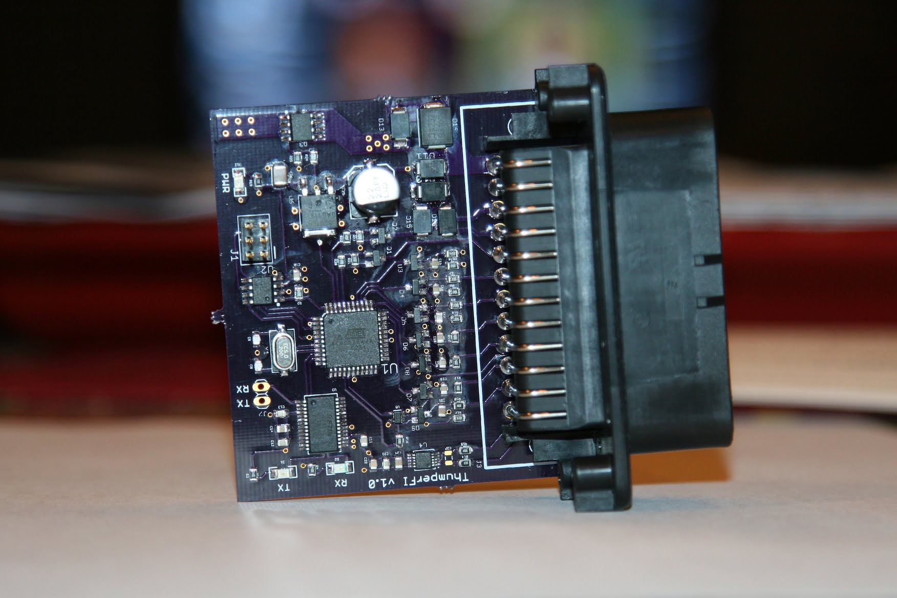
Kind of poor quality photo but shows the components the best.
While I was at home two weeks ago I was only able to able to test that it powered on – all of my other equipment was at school: my AVR ISP, oscilloscope, etc. So I attached a 9V across 12V_RAW and GND and the PWR LED lit up, so that was exciting.
When I got to school pretty much the first thing I did was set my work bench back up and hook ThumperFI up to my ThinkPad (i.e. “science” computer). It passed the visual inspection, the status LED on the ISP turned green which means my layout was correct. Then I opened up AVR Studio and checked if I could read the voltage and signature of my ATmega644A – which I could!
Now, there’s a decent amount of hardware to test on this thing and I was really busy last week so I spaced out the testing – I’ve since tested functionality of all major components (I haven’t done any intense testing like over-voltage, reverse-voltage, injector flyback, etc.) so I’ll summarize the results here before going in to detail about all of them:
- ATmega644A – functional, able to load programs, behaves as expected
- EEPROM – functional after modification
- FT232RL (USB) – non-functional, “device not recognized”, currently debugging
- ADC inputs – functional, including conditioned inputs like IAT, CLT and battery
- Injector, fuel pump and spark signal output – functional, behave as expected
- VR input – functional, converted 200mA sine wave to square at zero-crossings perfectly
- Kill switch input – functional, hardware debouncing works well
So other than USB, everything works! Now for the details.
EEPROM
EEPROM did not work, at all, right off the bat. So, I pulled up the schematic for the PCB and drew up a schematic for the EEPROM on my old prototype and noticed immediately that I had put a pull-down resistor on CS (Chip Select) instead of a pull-up (SPI CS is active low, so my chip was active all of the time). To fix this I cut the trace to GND and bridged the 10k resistor to the +5V cap terminal right next to it. Thinking I had fixed the problem I reloaded my test program and ran it again – no dice. I broke out my USBee DSA and carefully tapped off of the SPI lines and logged some data – everything was coming in to the chip correctly but there was no activity on the MISO line – strange. After examining and re-examining my circuits to make sure everything was the same (my test program worked on my prototype) I decided to ask my friend Mike for some help. He went through a number of checks with me based on what I gave him until he asked me what I had done with the ~HOLD pin. I told him it was just soldered to a pad connected to nothing. He said that the ~HOLD pin can tri-state if not pulled up and that can cause all sorts of issues – like the missing MISO signal I had. The SO-8 pitch is just big enough that I was able to bridge a 10k resistor across Vcc and ~HOLD and that immediately fixed the problem.
FT232RL
The second thing I tested after the ATmega644A was the USB capability. And it worked. Perfectly. So I assumed it was going to continue working and moved on to testing the EEPROM which, as described above, didn’t go so hot the first few times. Once I got the EEPROM working I wanted to see if I could output the values I had stored in the EEPROM on the screen using the USB connection. I hooked everything back up and it didn’t work. At all. I got the “device not recognized” message on Windows. I re-examined my FT232RL circuit and compared it to SparkFun’s circuit and didn’t really see anything wrong. Then I read FTDIs debugging tips and took note of the self-powered vs. VBUS powered section. I hadn’t really done either of those, more of some hybrid. And, even better, I had connected VBUS to +5V which makes no sense. So, I left VBUS disconnected and tried it again. No dice.
I ended up e-mailing FTDIs support and a very helpful guy pointed out the self-powered circuit (see Section 6.2 in this document) in the data sheet. So, I painstakingly soldered a 30 gauge wire to the FT232RL chip, made the 3.3V resistor bridge and tested it out. Still no luck. I have tried all of his suggestions as well as anything else I can think of:
- Make sure your USB cable is good – check
- Make sure your drivers are installed properly – check
- Restart – check
- Make sure all of your solder joints are good – check
- Plug in USB first, then power on and vice versa – check
So, after exhausting all of the options I could think of I ordered a new FT232RL chip from DigiKey and am waiting patiently to test that out (in case I roasted this one somehow – though the RXLED/TXLEDs still function…). I’m going to try the self-powered circuit first then if that doesn’t work maybe try the VBUS powered. I’ll need to make that decision before I get PCB v1.1 made.
ADC Inputs
There are 6 different analog inputs to ThumperFI:
- Battery (BATT)
- Intake Air Temperature (IAT)
- CooLant Temperature (CLT)
- Manifold Air Pressure (MAP)
- Throttle Position Sensor (TPS)
- Air-Fuel Ratio (O2)
TPS, O2 and MAP are simple inputs with no special conditioning (aside from current limiting resistors, Schottky protection and 0.1uF cap). The BATT, IAT and CLT all have a voltage divider giving me a known voltage or resistance. I tested the BATT and got 9V (which is what I was powering the system with at the time, minus the diode voltage drop). I tested IAT and CLT with a 10k resistor and 2.5V which is also what I was hoping for. All good on that front.
Injector, Fuel Pump and Spark
There are three outputs from ThumperFI (listed above) and all three of them work. Of course, I chased non-existent problems with the injector output for roughly an hour (turns out it was a programming issue, though I don’t really know what caused the issue because the changes I made in the code shouldn’t have actually done anything) – the pin wasn’t set as an output so it’s voltage was kind of floating around and wouldn’t drive the MOSFET. One interesting thing to note that I didn’t expect while debugging was that I would see the transistor base-collector voltage at the 10k pull-down resistor (makes sense, considering I was measuring at a trace connected to the base…). Regardless, it all functions on a basic level – I still need to test the Fuel Pump and Injector outputs under load conditions but it at least drives an LED.
Variable Reluctance Input
The VR input is kind of the most important part of this whole deal – if it doesn’t work I don’t have engine position and speed and can’t manage spark and injections. I saved this guy for last. I knew that the circuit worked before I made the PCB, I had built it using a DIP breakout for the MAX9924 and an actual trigger wheel (attached to a drill and holding the VR sensor). However, I was still a little nervous that for some reason it wouldn’t work BUT it did work, at least it works with a sine wave generated by my MyDAQ. I have a lawn mower engine in the garage with a trigger wheel mounted to it that I’m planning on testing it with (at speed) to confirm full functionality.
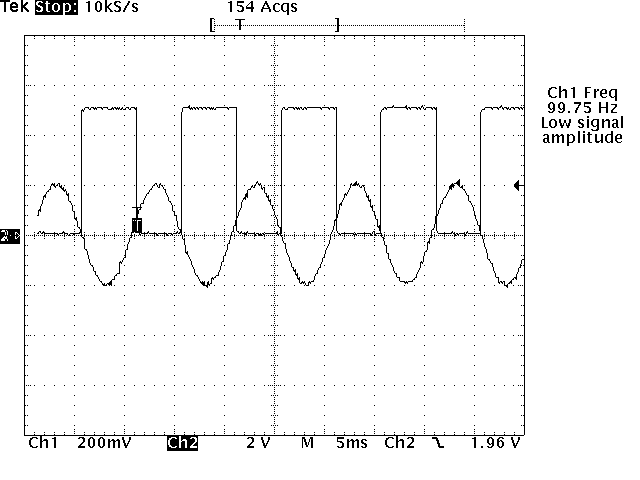
100 Hz, 400mA sine wave produces expected output. The MAX9924 is an active-low device so the falling edge indicates a tooth. Photo courtesy of TDS320 over RS232.
On a related note, I also figured out that I can just generate zero-crossings with any waveform and it will work – what that means is I can use the VR signal generator I’ve been working on with my Arduino and somehow level-shift the wave down and BAM I’ve got a functional, adjustable VR generator.
Kill Switch Input
Aside from the USB hardware, the Kill Switch input was the only untested portion of the hardware on this PCB. I grabbed a debouncing circuit from this guide. Works perfectly. It’s got a little longer RC time constant than I anticipated (honestly, I didn’t do the math so it’s probably exactly what it’s supposed to be) but I mean, hopefully you’re not just clicking the kill switch quickly wanting it to stop.
I might adjust this a bit in v1.1 but I’ll have to do some testing with it.
Other Lessons
I haven’t done a lot of extreme case testing yet (over/under-voltage, transients, etc.) and honestly I don’t really want to until I have an easier way of producing this board. In theory everything will function like it should, all of my inputs have Schottky diodes for transients, my regulator has a TVS with a clamping voltage of less than what my regulator can take, as well as a diode for reverse protection (and my regulator actually has quite a few built-in protections as well). My 22uF cap is rated for up to 100V which should pretty well cover any transients. Overall I’m hoping it’s a pretty solid design and I guess testing over the next few months will either prove or disprove that.
Now for some more pictures.

After multiple hours of soldering, it was born.

I mean, come on, I had to put my name somewhere on it.